Quantcast
Channel: Industrial
Viewing all 99 articles
Browse latest View live

How to reduce system cost in a three-phase IGBT-based inverter design

$
0
0

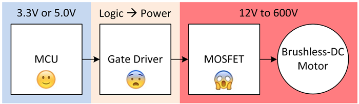
Most three-phase inverters use insulated gate bipolar transistors (IGBTs) in applications like variable-frequency drives, uninterruptible power supplies, solar inverters and other similar inverter applications. Each phase of a three-phase inverter uses a high- and low-side IGBT to apply an alternating positive and negative voltage to the motor coils. Pulse-width modulation (PWM) to the motor controls the output voltage.

The three-phase inverter also uses six isolated gate drivers to drive the IGBTs. Apart from the IGBTs and isolated gate drivers, three-phase inverters include DC bus voltage sensing, inverter current sensing and IGBT protection like over temperature, overload and ground fault.

Cost and performance are challenging trade-offs in many end applications like heating, ventilation and air conditioning (HVAC), solar pumps and appliances.

So what are the best ways to save bill of materials (BOM) cost without compromising system performance? Here are some tactics:

  • Combine the high- and low-side drivers into a single package. A three-phase inverter requires six IGBT gate drivers. You can use individual gate drivers for each IGBT, but a dual-channel gate driver helps with design flexibility and reduces BOM cost.
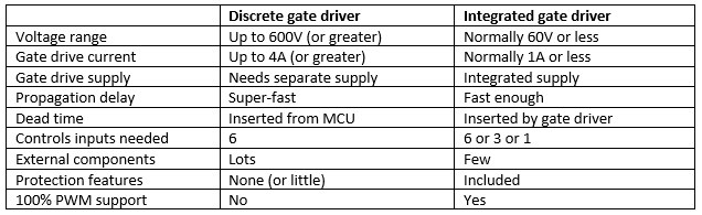
  • Power the gate drivers with a bootstrap. Needless to say, any high-voltage inverter application will need isolation between the primary and secondary side of the gate driver for reliable operation. The isolated gate drivers may need different supplies for the high and low sides. Instead of using six different isolated supplies for a three-phase inverter, a bootstrap power supply reduces the power-supply requirements to only one, thus reducing total BOM cost and board space.
  • Protect the IGBTs using simple comparators. You can achieve simple overload and short-circuit detection by sensing the current and using window comparators. The comparator output can disable the IGBT gate drivers with the DISABLE function.

TI’s newly released UCC21520 is a reinforced isolated dual channel gate driver. With best in class propagation delay of 19ns (typical), programmable dead time and wide voltage ranges make it really suitable for such inverter applications.

Apart from the IGBTs, the IGBT gate drivers and current sensing play a major role in determining the cost and performance of the three-phase inverter stage. Consider the following tactics save BOM in current sensing circuit:

  • Shunts. Instead of bulky and costly hall and fluxgate current-sensor modules, shunts optimize the cost and space of sensing circuits. Current transformers are also considered but have issues with linearity and performance compared to shunt.
  • In-phase current sensing for better sensing performance (compared to leg current sensing). In-phase current sensing means that there is a constant motor current flowing through the shunt (compared to a noisy switching current in leg current sensing), regardless of which IGBT is switching. Also, it is easy to detect terminal-to-terminal shorts and terminal-to-GND shorts. You can also use two shunts for cost optimization and calculate the current of the third phase in software by using data from the other two sensing circuits.
  • Consider using isolated amplifiers along with a shunt instead of a hall current sensor. Using isolated sigma-delta modulators for current sensing requires digital filters implemented in software or hardware. An isolated amplifier enables interfacing with low-cost microcontrollers with a built-in SAR ADC.
  • Simple overcurrent protection. High-bandwidth isolated amplifiers and comparators with fast response times (<5 to 6µs) enable fast overcurrent protection for inverters, thus allowing you to use cost-effective gate drivers in your system.

AMC1301 is TI’s newly released precision reinforced isolated amplifier. It is optimized for direct connection to shunt resistors and supports accurate current control. The high linearity and low temperature drift of offset and gain errors of the AMC1301 results in system-level power savings and lower torque ripple. With 3µs delay and detection feature of missing high-side supply makes is suitable for motor drives applications.

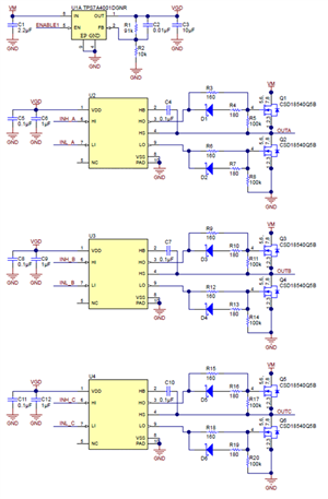
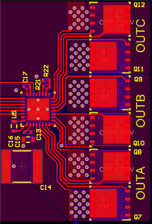
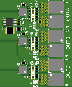
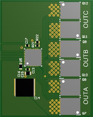
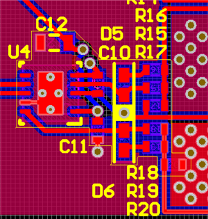
The new TI Designs Reference Design for Reinforced Isolation 3-Phase Inverter with Current, Voltage and Temp Protection (TIDA-00366) provides a reference solution for a three-phase inverter rated up to 10kW. Figure 1 is a high-level block diagram.

Figure 1: High-level block diagram of TIDA-00366

The design includes the UCC21520 reinforced isolated dual-IGBT gate driver, AMC1301 reinforced isolated amplifier and TMS320F28027 MCU. A lower system cost is possible by using the AMC1301 to measure motor current (interfaced with the MCU’s internal ADC), with a bootstrap power supply for the IGBT gate drivers. The inverter is designed to have protection against overload, short circuit, ground fault, DC bus undervoltage and overvoltage, and IGBT module over temperature.

What techniques do you use for saving the BOM? Tell us.

Additional Resources:

  • White papers:

Accuracy? Resolution? Arc minutes? How to take charge of your motor control design

$
0
0

Imagine your commute this morning in your car. The traffic light turned green, and you pushed the accelerator as soon as you could. Your car responded within seconds and you continued on toward the office. But behind the scenes, inside your car, there was a lot more happening. Let’s take a look.

When you press the pedal, the motor does its best to provide the necessary torque to your car through the shafts. The traction motor drives your vehicle forward. This motor (typically a three-phase synchronous motor) is controlled by complex circuitry that consists of several transistors, as well as motor driver, protection and feedback control. The feedback control signal comes from motor position sensors (see Figure 1). These sensors give an analog angle output signal (remember, all real-world signals are analog). This continuous analog signal is converted into the digital domain with the help of an analog-to-digital converter (ADC). Ideally, you could break the continuous analog signal into an infinite number of digital steps, but in the real world, the quantization of an analog signal by the ADC happens in a finite number of steps leading to an error, known as quantization error. Here is where the terms “accuracy” and “resolution” kick in.

Figure 1: Typical system block diagram of a motor-control system in a vehicle

Accuracy

Take as an example a 12-bit resolver-to-digital converter (RDC). Over one revolution of a shaft, the output of the converter has 212 = 4,096 digital codes. In the motor-control world, step size is usually defined in terms of arc minutes or arc seconds. There are 60 minutes in one degree and 360 degrees in one revolution. Thus, over a circle, you have 360 × 60 = 21,600 arc minutes. Since there are 4,096 digital codes, each division is spaced by = 21,600/4,096; that’s 5.27 arc minutes. 5.27 arc minutes corresponds to one least significant bit, or 1LSB. Thus, even when the input angle (a continuous signal) is 100% accurate, the output digital code cannot move by more than 1LSB (or 5.27 arc minutes) before the next code. The RDC specifies this accuracy number by taking into account offset, gain and linearity errors. For reference, the typical accuracy specification for a brushless resolver is 10 arc minutes. The typical error for the entire resolver system, adding the sensor and the conversion error, is approximately ±15.273 arc minutes (10 arc minutes for the resolver sensor and +5.273 arc minutes in my example). These numbers will help us select the appropriate sensor solution for the system, which are typically constrained by these specifications.

Resolution

So, what does resolution mean? “12-bit” resolution means 212 distinct output codes over a 360-degree angular rotation. The actual resolution is simply the number of bits available at the output of the RDC; note that not all of these bits are noise-free. The effective resolution refers to the true “useful” bits from an analog-to-digital conversion, taking into account the signal noise. These are the effective number of bits (ENOB). ENOB is often confused with the resolution stated in the product data sheet.

What does 1 LSB mean?

So far, we’ve reviewed what accuracy and resolution means. Now, let’s take this knowledge and apply it to a system where accuracy and resolution are usually specified in terms of LSBs. Are you wondering how to make sense of an LSB from a systems context? First, let’s look into what 1 LSB translates to in the motor control world, relating to arc minutes and degrees. Here are two examples, 12-bit and 10-bit:

In the 12-bit world, 1 LSB equates to:

1LSB = 360 ÷ 212 = 0.087 degrees = 5.27 arc minutes = ±2.64 arc minutes = ±0.04395 degrees

Similarly, in the 10-bit world, 1 LSB equates to:

1LSB = 360 ÷ 210 = 0.351 degrees = 21.09 arc minutes = ±10.54 arc minutes = ±0.1757 degrees

Conclusion

Isn’t it exciting to see what happens behind the scenes in your car? Accuracy and resolution are the fundamentals of selecting the appropriate sensing solution for your specifications. When accuracy is better than resolution, the converter’s transfer function is precisely controlled over the number of bits of resolution.

Leave a comment below or visit the TI E2E™ Community Automotive forum to join others talking about rotary position sensing.

Additional resources

EtherCAT and C2000™ MCUs - real-time communications meets real-time control

$
0
0

We heard you and now we want to help you! We released our first DesignDRIVE industrial communication reference design (TIDM-DELFINO-ETHERCAT) to help ease your development of IEC 61158-compliant EtherCAT slave nodes based on our C2000™ real-time control microcontrollers (MCUs).  Since C2000 MCU DesignDRIVE has the perspective of those developing for industrial real time control; we have seen the popularity worldwide for the support of EtherCAT.  The demand appears to fall into two categories primarily: a) when required to interface to a larger/factory-wide EtherCAT network and b) when selected to replace CAN networks to fulfill  higher bandwidth and lower latency node to node communication requirements in industrial machines.

 There are some very good reasons why EtherCAT is a natural fit for C2000 MCUs in industrial automation applications. First, both have been designed for real time applications.  Most EtherCAT slaves rely on hardware gates, versus a software approach, to handle the real-time data link layer thus enabling node-to-node packet latencies in the range of one microsecond. That latency makes EtherCAT one of the best protocols for addressing real-time communication needs.  C2000 MCUs, have been built for real-time control.  This is evident when you look at C2000 MCU features such as zero wait-state accesses to a 3.5 MSPS ADC with hardware post processing, 50ns PWM trip time from an overcurrent event and a 95ns floating point Park transform time.  Both architectural philosophies reduce the CPU loading thus reducing the time/cycles needed to perform the main communications or control loops. 

Next, both EtherCAT and C2000 MCUs place a premium on the importance of reducing overall system cost.  That’s why the required memory to run an EtherCAT slave stack is kept to a minimum. Likewise, the C2000 MCUs, especially for industrial drives applications, integrate an unprecedented number of drive functions on-chip such as the absolute encoder master, sigma-delta filters, over-current comparators, current loop accelerator, high performance ADCs and DACs, clockwise-counter clock- wise (CW/CCW) inputs, pulse train output (PTO) and program storage. In addition, the mathematically enhanced C28x MCU instruction set has been optimized for real-time, computational code and results in memory-saving high-density code.

Because of the common philosophy placing priority on real-time capabilities and the benefits of using them together, C2000 MCUs and EtherCAT slaves are a natural fit and commonly found together in applications like high performance industrial servo motor control.

Why did you base the EtherCAT reference on the ET1100? 

The answer is quite simple.  To us, the ET1100 ASIC from Beckhoff Automation GmbH, the inventor of EtherCAT, is the “gold standard” for compliance to the EtherCAT slave implementation and use model.

Whether a commercially available EtherCAT slave node is implemented in an FPGA or ASIC, the bases for most designs are derived directly from the Beckhoff or are built to behave compatibly to the Beckhoff design.  We want our reference solutions to be held to this same standard and extend seemless compatibility to existing EtherCAT networks, even allowing the slave stack to leverage either 16 bit parallel or SPI interfaces on the ET1100 as is. The DesignDRIVE EtherCAT Slave software solution provided as part of the TIDesign reference design, as well as part of future DesignDRIVE EtherCAT releases, will always strive to be compatible with the gold standard.  

Start developing your next design today. Visit the below links for more information: 

How motor drivers aid in an automobile’s “limp-home” mode

$
0
0

Have you ever had the check engine light come on while you are driving and your vehicle’s operation is limited? This can happen when there is an issue with the transmission; to protect itself, the vehicle might stay in first gear. Or it can happen when a piston is not firing, the vehicle is overheating or the tire pressure is low. Typically your vehicle will give you some indication in the dashboard, as seen in Figure 1.

Figure 1: Cluster Vehicle Diagnostics  

A vehicle’s limited operation after a system-level fault is called “limp-home” mode. Limp-home mode is a secondary programming feature embedded in the vehicle’s transmission and engine-management computers. These computers monitor and control hundreds of system-level features constantly. When a certain component senses a fault, the computers begin operating that component in a range safe enough to stay below the limits of the fault.

One benefit of engine and transmission systems moving toward electric motors for many actuation needs is that the electric motor can be controlled by the electric control system with more intelligence to support limp-home mode, whereas previously belt-driven actuators constantly ran off of the belt and had no fine control. A good example is the water pump, as seen in Figure 2, which is pivotal in cooling the engine. If there is damage to the electronics driving the water pump, then it is better to drive with much less torque and speed until the pump can be repaired. Obviously, the vehicle won’t be able to go as fast, but it will also not need as much coolant.

Figure 2: Electric Water Pump

The DRV8305-Q1 offers limp-home mode support by allowing on-the-fly configurability while driving a brushless DC motor. In the water-pump example, if one of the power MOSFETs driving the motor has an overcurrent situation, the DRV8305-Q1 uses flags/warnings through the serial peripheral interface (SPI) port instead of shutting down the driver so that control transfers to the microcontrollers (MCUs). Similarly, implementing slew rate/gate drive current control (IDRIVE) during motor-drive operation reduces switching losses for an overheating system; the side effect of this is reduced motor torque.

As vehicle suppliers push more towards safe and intelligent operating components, it is important for system designers to use the smartest devices. What is your experience designing with brushless DC gate drivers? Sign in and comment below.

Additional resources

Know your electromagnetic compatibility requirements for designing industrial drives

$
0
0

Variable-speed and industrial drive design engineers need to know electromagnetic compatibility (EMC) immunity and electromagnetic interference (EMI), as well as isolation safety requirements. Do you know your requirements? Each end-equipment design has to meet its own standards, which ensures that the product is compliant and safe for use in the desired end equipment category and environment.

The corresponding end-equipment standards for variable-speed drive systems, issued by the International Electrotechnical Commission (IEC) are the IEC 61800-3 for EMC and EMI and IEC 61800-5-1 for system safety requirements, which includes isolation. The EMC and EMI requirements specified in the IEC 61800-3 standard depend on the category under which the variable speed drive falls. The category ranges from C1 to C4 and specifies the maximum rated voltage of the variable speed drive and the environment it can be installed and used. The maximum rated voltage of the drive can be less than 1000V or more than 1000 V. There are two environments:

The first environment refers to using variable speed drives in domestic premises like houses or office buildings which are supplied from the public grid. The second environment specifies requirements for use in an industrial area powered by a dedicated transformer that supplies 3-phase voltages such as 480V, 560V or 690VAC. In this blog post, I will focus on category 2 and 3 and direct you to a corresponding training video series.

Drives for category C2 have rated voltages below 1000V, fur use in the first environment, but be neither plug-in nor movable and installed by a professional. Drives for category 3 have rated voltages below 1000V too, but are restricted to use in the second environment only.  

Semiconductors have their own specific EMC and isolation standards at the component level. Some examples are shown in Table 1.

Table 1: Component-level semiconductor standards

How do EMC immunity, EMI and isolation requirements apply to industrial drives, and what do the tests look like? Figure 1 shows a simplified architecture of an industrial drive, partitioned into various subsystems with interfaces and connectors accessible outside the cabinet. EMC immunity test signals like surge, electrical fast transient (EFT) or ESD are applied to the interface connectors of each subsystem. Typical subsystems with accessible interfaces or connectors include the communication, user input and output (I/O) interface, the position feedback interface, the power interface and the mains AC power input.

Figure 1: Example EMC immunity test signals in an industrial drive

Each interface or port has to pass the corresponding EMC immunity requirements and EMI and isolation requirements. Especially semiconductors interface ICs like Ethernet PHYs, RS-485 transceivers or isolated gate drivers have a major impact on passing system-level standards. Therefore the EMC immunity, EMI or isolation performance on semiconductor component level as shown in table 1 becomes a key selection criterion.

To learn more about EMC, EMI and isolation standard requirements for industrial drives, and how to design and test standards-compliant hardware, watch Section 1 of the training video series.

EMC immunity

Let’s look at EMC immunity requirements and test methods. IEC 61800-3 specifies EMC immunity requirements like voltage level and pass criteria and refers to the IEC 61000-4-x standard, which describes the test methods and test setup for ESD, EFT and surge. The EMC immunity requirements are higher for the second environment and lower for the first environment. Hence we focus on second environment. Figure 2 shows an excerpt of IEC 61800-3 EMC immunity requirements for the second environment. 

Table 2: IEC 61800-3 EMC immunity requirements for second environments

Each port need to pass specific over-voltage phenomenon, specified in a standard like IEC 61000-4-4 for fast transient burst (EFT) at a voltage level of +/- 2kV.

How can we validate drive has passed the test? Therefore the performance acceptance criterion as shown table 2 is a very important factor to validate end-equipment-related EMC tests.

Criterion A specifies that the performance of the drive must not be impacted during or after the EMC test.

Criterion B specifies that temporary performance degradation is only acceptable during the duration of the EMC test. After the test EMC test the drive must operate with full performance without any manual intervention.

Criterion C specifies that temporary loss of function or performance is acceptable during the test, and allows manual intervention like a power cycle or hardware reset to get back to normal operation with full performance.

Unlike most semiconductors, which are typically validated according to criterion C, end equipment must meet at least criterion B or A, where A specifies that the system must maintain the specified performance even during an EMC event. For many vendors immunity against fast transient burst (EFT) per IEC61000-4-4 is the most important EMC immunity test to proof the robustness of an industrial drive. This is due to the fact that impulse noise coupled into cables or printed circuit boards through the inverter PWM switching voltage has a similar impact on the drives performance than a fast transient burst (EFT).

How do you design EMC standard compliant subsystems? TI reference designs for industrial drives are designed to meet EMC immunity requirements for industrial drives. For example, Universal Digital Interface to Absolute Position Encoders Reference Design implements an EMC-compliant RS-485 interface for four- and two-wire encoders. The reference design exceeds the IEC 61800-3 requirements by passing the required test voltages by a factor of two.

To learn more about EMC immunity requirements, test setup and hints on how to design industrial IEC EMC-compliant hardware based on a position encoders reference design, watch Section 2 and Section 3 of the training video series.

EMI

The IEC 618000-3 also specifies emissions requirements for variable-speed drives and refers to the standard CISPR 11 class A and the equivalent European Standard EN 55011 class A. standard for the specific test setup. CISPR is the short form for the Comité International Spécial des Perturbations Radioélectriques. The radiated emissions are measured in the frequency band from 30MHz to 1GHz. For industrial equipment which falls under category 2 or 3 per IEC61000-3, the limits for the electric field strength component quasi-peak in decibels (microvolts per meter), as shown in Table 3. 

Table 3: Limits for electromagnetic radiation disturbance in the 30MHz to 1000MHz frequency band (see IEC 61800-3, Table 15)

The EMI/EMC Compliant Industrial Temp Dual-Port Gigabit Ethernet PHY Reference Design is a good example of a design that passes IEC 61800-3 EMC immunity requirements and exceeds EN 55011/CISPR 11 radiated emission requirements for Class A by 4.3dB.

To learn more about EMI, test setup and how to design industrial EMC- and EMI-compliant hardware, watch Section 4 of the training video series.

In my next post, I’ll examine specific isolation requirements for variable-speed designs.

Additional resources

How to avoid motor and system overvoltage using AVS technology without external components

$
0
0

In the world of advanced and complex technology, system protection becomes a very important aspect of delivering reliable, robust and high-performance equipments for both industrial and automotive that’s protected against malfunctioning due to overvoltage or overcurrent.

For motor-based systems, there must be an energy transferred to the motor in order for the motor to spin. The energy transmitted from a power supply to the motor generates angular motions that under some uncertain conditions might return that energy back to the power supply. This returned energy can aggravate system overvoltage to cause device failures and even sometimes destroy motor-drive stages. These failures are due to a condition called voltage surge.

Let’s examine which conditions cause these device failures. For systems requiring a motor, two types of energies facilitate system operation: inductive energy and mechanical energy.

Inductive energy occurs when the current flowing in the inductance of a motor continues to flow through the intrinsic body diode of the MOSFET, which eventually causes an increase in the supply voltage. Figure 1 shows what happens when an inductive energy is active.

Figure 1:  Inductive Mode Voltage Surge

You can see in Figure 1 on the left that current is flowing from S1, then S6, which makes the inductive energy return to ground. On the right, in active tri-state mode, if the current flows from S2, then to S5, and the inductive energy is dumped in the supply voltage (VCC).

To prevent this generated inductive energy from returning to the power supply, TI integrated circuits (ICs) come with Anti-Voltage Surge (AVS) technology to monitor both high- and low-side current. See Figure 2.

Figure 2:  Inductive AVS Implemented

Mechanical energy is caused by an unexpected decrease in speed, which might cause the supply voltage to drop lower than the back electromagnetive force (BEMF) voltage. In this scenario, the motor works as a generator and current flows back to the power supply.

AVS prevents these conditions from occurring, thus preventing energy from being transferred from the motor back to the power supply. AVS also protects other devices connected directly to the power supply. This is significant, because it enables you to remove devices designed to protect against overvoltage. The elimination of these extra protection components helps simply the design, minimizes board space and improves system performance. In addition, it saves design time and reduce overall system cost.  

AVS monitors speed commands and limits the value of the supplied voltage from exceeding the motor’s BEMF. Upon the detection of a voltage surge, AVS quickly reacts to maintain the desired output amplitude during system operation.

AVS is available in many Texas Instruments motor driver ICs, including the DRV10983, DRV10975, DRV10963 and DRV10964. Figure 3 shows the spin of the DRV10983 motor driver with AVS both enabled and disabled.

Figure 3:  AVS Wavefroms (AVS Applied vs AVS Not Applied )

Design protection is very important in today’s complex technology world.  AVS, a technology developed from Texas Instruments, monitors and prevents unwanted conditions to the system. These conditions can cause overvoltage, failure and sometimes destroy the system. A motor-based design is simplified, made more robust and reliable by designing and utilizing products that support AVS technology to help prevent overvoltage from occurring. What is your experience designing with brushless DC motors? Sign in and comment below.  

Additional resources


The other motors in electric vehicle systems (part 2)

$
0
0

In the previous installment we had just discussed EV auxiliary motor systems.  Most of these are low voltage and low to medium current three-phase brushless DC motors which can – with the right expertise – be controlled without mechanical rotor magnetic position sensors (sensorless).  These three-phase motors are energized by a three phase inverter, which switches DC voltage through three parallel legs to ground.  Each phase of the motor is connected to the midpoint of a leg, allowing for current flow through a phase between Vdc and ground.

The components used to energize each phase of the three phase motors in the inverter system are MOSFETS. As seen in Figure 1 below, six MOSFETs are arranged in a totem pole fashion, creating three half bridges to switch each coil to the DC voltage and ground. 

Figure 1: Integrated Three Phase Gate Driver (DRV8305) with external FETs 

Unlike low voltage MOSFETs, High Voltage/Current FETs cannot be driven directly from the microcontroller (MCU). Due to the high threshold voltage and high amount of capacitance that is parasitic to the FET (typically >100pF.), a driver IC must be used to drive the gate of the FETs (typically termed gate driver). Modern gate drivers in (1kW three phase motor systems) integrate many features that are important to the overall system’s reliability and performance. These key features are based on protection, configurability, build of material / board size reduction and motor control performance. The DRV8305-Q1 is best in class in each one of these features.

Since MOSFETs are the key components energizing the three phases, they are the most critical to be protected. The DRV8305-Q1 offers multiple layers of protection for the overall system by having integrated VDS and VGS monitoring of the external FETs, on chip thermal measurement, three integrated current shunt amps to monitor current flow through the FETs, MCU watchdog, power supply monitoring for under and over voltage and shoot through protection with smart gate drive. Out of each level of performance, smart gate drive is where DRV8305-Q1 differentiates itself from other gate drivers. It offers three levels of MOSFET cross conduction or shoot through protection by allowing the user to set a minimum dead-time (time between high side and low side switches being on) and by implementing a strong gate pull down to prevent dv/dt conduction. For further details on smart gate drive, read our app note “Understanding IDRIVE and TDRIVE in TI motor gate drivers.”

Along with protection the DRV8305-Q1 integrates many high performance features that will eliminate many devices and material that is seen on a typical BOM. The first of those is configurability and diagnosis communication through a serial peripheral interface (SPI). Each one of the failure mechanisms mentioned above will be reported on the SPI port when there is a failure. The SPI port can also be used to program or configure many features. A key feature is the gate drive current, eliminating the need for resistors on the gates of the MOSFETs. It can program the current as low as 10mA and as high as 1.25A, allowing users to tune for optimal gate drive and EMI performance. Other key features that are programmable are the gain, bias and blanking time of the current sense amps.

Lastly, the DRV8305-Q1 is great in improving motor performance by aiding in each control algorithm and method from simple trapezoidal to sinusoidal FOC. This is made possible by the single, three or 6 channel pulse width modulation (PWM) options and high performance current shunt amps. To aid in FOC, each current shunt amp must be able to make a fast and accurate measurement of the current in each phase leg. The DRV8305-Q1 offers current sense amp calibration via the SPI port to minimize inaccuracy related to offset voltage.

Learn more: 

Understanding isolation requirements for industrial drives

$
0
0

In my last blog post, we looked at electromagnetic compatibility (EMC) and electromagnetic interference (EMI) requirements for industrial drives.

Why would we develop hardware with isolation? We can isolate sensitive measurement from noisy supply domains for improved accuracy, reduction of common mode noise although isolation may not be required due to safety. We call this functional isolation.

The most obvious reason for isolation is the safety aspect to protect against electrical shock. A system must ensure protection from hazardous voltages. If these voltages are present in a system isolation is mandatory.

There are two levels of isolation:

  • Systems with basic isolation provide a single level of isolation with basic protection against electric shock.
  • Systems with double isolation are comprised of two independent layers of basic insulation. Another independent insulation is added in addition to the basic insulation to ensure protection against electric shock in the event of a failure of the basic insulation.

Systems with reinforced isolation provide a single insulation system that provides a degree of protection against electric shock equivalent to double insulation under the conditions specified by the corresponding standards.

For variable speed drives the relevant standard is the IEC 61800-5-1. The corresponding semiconductor level standards are for example the IEC 60747-5-5 for optical isolators and for capacitive/magnetic isolators the VDE0884-10/11 and the draft version of IEC 60747-17. What are key parameters specified? The IEC 61800-5-1 specifies the level of insulation required between high voltage and conductive parts/equipment surface, in terms of:

  • Transient overvoltage (corresponds to VIOTM)
  • Surge voltage (corresponds to VSURGE)
  • Creepage
  • Clearance

This is depending on depending on:

  • Basic or reinforced isolation is required
  • System voltage
  • Working voltage (corresponds to VIORM)
  • Overvoltage category
  • Pollution degree
  • Package material

Table 1 shows an overview on isolation terminology.

Table 1: Isolation terminology

Let’s have a look at a hardware design example of an industrial drive’s 3-phase AC inverter. The AC inverter is typically fed from the 3-phase AC grid. The amplitude of the 3-phase AC typically specifies the DC-link voltage. To isolate the microcontroller from the power stage, isolated IGBT gate drivers as well as isolated phase current and voltage sensors are used.

How can we retrieve the isolation voltage requirements from the AC or DC input voltage?

The IEC61800-5-1 specifies the corresponding electrical parameters like temporary overvoltage, impulse surge voltage, minimum clearance and creepage for basic of reinforced isolation based on the system voltage along with other parameters like category, pollution degree and altitude. The relevant system voltage per IEC61800-3 is for example 300V, 600V and 1000V. The system voltage specified by the vendors must not be lower than the relevant IEC61800-3 voltage.

For example for a system specified for 830Vrms, the IEC61800-5-1 requirements for 1000Vrms will be valid. The maximum sinusoidal peak voltage to tolerate for 60s is 6.2kVpk, the maximum surge voltage is 12kVpk and the maximum peak working voltage is 830Vrms.For systems to pass IEC61800-5-1 the temporary peak and surge voltages for reinforced or basic isolation depend on the system voltage. Note that for semiconductor isolators the relevant components standard requires isolators with reinforced isolation pass at least 10kV surge.

How do we select the right semiconductors and what are the hardware design considerations to meet the isolation requirements? The Isolated IGBT Gate Driver Evaluation Platform for 3-Phase Inverter System Reference Design is a good example for a reinforced isolated IGBT gate driver evaluation platform for 3-phase inverter systems. This design supports up to 1500Vrms working voltage. The design has been tested with motors up to 22kW and exceeds the IEC61800-3 EMC immunity for power interfaces with 8kV ESD contact discharge and 4kV EFT by twice the required voltage level. Isolation requirement, terminology and a TI hardware design example are explained in the training video series Section 5: Isolation requirements in industrial drives.

If you’re ready to learn more, watch the training series Design considerations for EMI, EMC immunity and isolation requirements or download the corresponding Motor Drive & Control system reference designs.

If you would like to see more on specific topics related to design consideration for EMI, EMC immunity and isolation requirements in industrial drives, please post a comment below.

Additional resources:


The other motors in electric vehicle systems (part 3)

$
0
0

The switching of the three-phase inverter needs to be controlled by digital logic – typically a programmable microcontroller (MCU) - to regulate the torque or velocity of the motor while maximizing the efficiency (required torque with minimum current usage). With the use of hall sensors on the motor it is reasonably straight forward to control a BLDC motor using a six-step (trapezoidal) commutation control technique with limited digital logic resources (a very small programmable MCU or even a hard coded ASIC). 


 This six-step approach has some limitations surrounding torque inefficiency:

  • The six-step trapezoidal switching is producing stator magnetic fields in only one of six orientations, while the motor efficiency would be maximized if the stator magnetic field could be created in a specific synchronized orientation to the constantly moving rotor magnetic field.
  • The switching between these six states causes ripple – a momentary reduction and then correction – of the torque being produced by the motor. This affects the quality of the velocity control and can even impact audible noise.
  • Dynamic performance (ability to adjust torque creation to meet the instantaneous load requirements) is then affected.
  • Efficiency is further reduced in many motors by these trapezoidal (square) voltage waves being applied to motors which are typically wound (primarily for production cost reasons) to produce sinusoidal back-emf voltage.  Most motors run more efficiently and effectively when driven with sinewaves instead of square waves.

An approach that works better for most of these motors is called Field Oriented Control (FOC).  In FOC, you can produce a stator field that is oriented and synchronized to the rotor field, which maximizes torque production.  The transition between stator states is smooth, removing torque ripple and improving the dynamic performance of the system.  The voltages seen by the motor phases are sinusoidal, enhancing efficiency.  FOC isn’t that much more complex than six-step BLDC. It measures at least two phase currents instead of one bus current; does some additional math calculations; two proportional-integral (PI) current controllers instead of one; and a few more calculations for the pulse width modulation (PWM) generation.

However, there is the issue of the rotor sensor.  The hall sensors used in six-step BLDC do not give enough accuracy on the position of the rotor magnetic field location for FOC. Further, hall sensors have some upfront costs (including additional wiring and voltage requirements), as well as lifetime costs due to their low reliability and high system failure rate.  Additionally, some applications simply can’t use hall sensors due to mechanical limitation (e.g. compressors).  A solution could be to use a different type of rotor magnetic sensor.  Digital encoders (often used in high precision servo drives) and analog resolvers (often used for the EV propulsion motor) give the resolution required for FOC, but are expensive and impractical compared to simple hall sensors.  The only solution then is Sensorless FOC.

Sensorless FOC rely on software algorithms to estimate the rotor magnetic field position (and often rotor velocity) based on the currents and/or voltages in the inverter.  Sensorless rotor position estimators (or observers) have been theorized, developed and in use for over 25 years. But their practical implementations have pretty much been constrained to those companies with extensive investment in creating this expertise (AC drives, industrial motor control, some advanced appliance and automotive).  At TI, we have been providing software libraries and system examples of Sensorless FOC for 20 years.  Through this process, we have realized some significant limitations of the conventional Sensorless FOC solutions available from semiconductor suppliers (including our own).  Therefore, we created a new software observer (FAST) and control solution (InstaSPIN-FOC) which solves these challenges.

InstaSPIN-FOC capability is made available through use of an on-chip library integrated into three members of TI's 32-bit real time Piccolo™ MCU controllers.  Piccolo MCU devices are widely used in industrial and automotive applications and are available in industrial (-40 to 105C) and AEC automotive Q100 (-40 to 125C) temperature grades. The quickest way to get started spinning your motor is to purchase an InstaSPIN-FOC enabled three-phase motor control evaluation module of the appropriate voltage and current level. 

Learn more:  

How to create a dynamic power solution for stepper motors, relays and LEDs

$
0
0

As you can see from my previous blog, my dad has always been a great source of inspiration and knowledge for me. There is one piece of advice that keeps coming back to me: “Measure twice and cut once.” However, as engineers, whenever we are challenged to design a control or power circuit for stepper motors, LEDs and other peripherals, we like to adapt the system to specific rules and conditions. We are essentially measuring twice, but only for that specific set of conditions. Any changes after the fact would only mean additional costs and time for evaluation, which can be a big pain for any project. Or as my dad would say: “You already made your cut, you can’t take it back!”

So what happens when you need a solution for multiple systems or configurations? How can you make sure that you maintain a balance between having a system that can power a motor, but also gives you the flexibility to add other high-voltage devices after your design is done? I recommend starting your design by using a module or subset of the system, which you can later scale.

Interfacing flexibility

The first thing you have to do is make sure that you can connect your power driver at will. While it is a good idea to choose a host controller with enough general-purpose input/outputs (GPIOs) to drive your outputs, implementing a control scheme or program becomes increasingly difficult, as each GPIO pin has its own call and action to execute. This is where serial interfaces become handy. Most processors have a slew of internal interfaces, as you can see in Figure 1. These interface modules can control memory or external sensors, and even communicate with other processors.

Figure 1: MSP430™ internal block diagram

For our system, however, the choice is simple. As I mentioned in the intro, we are making this system to drive multiple peripherals including stepper motors. For Stepper motors we need to make sure we supply a sequential and synchronized output from the host.

Figure 2: SPI master-slave connection

Interfaces like Serial Peripheral Interface (SPI) and I2C give you the advantage of having a clock signal coming from the host or master (as shown in Figure 2), with the ability to expand by sharing the serial data and clock lines. For the sake of your design, however, you want to keep costs low, since a solution with a high number of motors and LEDs would need multiple iterations.

Some motors, LEDs and other devices may not benefit from having the internal serial interface as a processor. In those cases, you can employ a serial-to-parallel converter such as the SN74HC595 shown in Figure 3. This device helps channel data sequentially to the outputs. I picked this part for my design because it’s easy to use, low cost, and enables designers to stack or daisy-chain similar devices. Any other serial-to-parallel device can also help complete the task, such as the SN74HC164 or TCA9539.

Figure 3: SN74HC595

Driving high voltage and high current

Unfortunately, you cannot simply drive a high-power load from a host microcontroller. You can, however, apply a FET to lower the overall current demand from the processor. This is in fact one of the more popular threads in design forums, and the main reason why the “Interfacing the 3-V MSP430 to 5-V Circuits” application note is very popular. If you take a page from this app note, you’ll see that the ULN2003A is a simple solution.

Figure 4 showcases how the MSP430 microcontroller and ULN2003A can drive a 12V logic rail along with some motors and LEDs. This works out great because the ULN2003A can handle voltages up to 50V and currents up to 500mA/channel, which gives you ample range for motors and LEDs.

Figure 4: Connecting the MSP30 to high voltage and high current loads

Putting it all together

Now that you have everything you need, you can connect your MSP430 MCU, SN74HC595, ULN2003A and a CSD17571Q2 to create a flexible power structure that’s scalable in multiples of eight channels, as shown in Figure 5.

Figure 5: Our dynamic driver system

You can use this architecture to create complex systems such as an air conditioner, an LED display matrix, or even a robot with multiple lights and motors. You can also create multiple versions of the same design with added features or functionality, such as extra displays or motors, as shown in Figure 6.

Figure 6: Scaling our power driver to accommodate more peripherals

Because you kept the design at a comfortable scale, you can now expand or reduce your features based on your application requirements, or recycle the same structure to come up with other applications that need high voltage, high current or both. And because you only chose the lower-cost alternatives, you can ensure that your board remains cost-effective, even with multiple iterations.

This is such an easy-to-use and flexible design, that we took this idea and made a BoosterPack out of it. But it is just one of the many different ways that you can drive high-power peripherals such as stepper motors and LEDs. What other architectures can you think of? Please let me know in the comments.

Additional resources

Increase the reliability of industrial drives with an EMC-compliant resolver sensor interface based design

$
0
0

Resolvers provide accurate and high-reliable position feedback in industrial drives like servo drives, especially in harsh industrial environments with dust and temperatures above 150°C. A resolver is an absolute mechanical angle sensor and operates as a variable coupling transformer. This means that the amount of magnetic coupling between the primary winding and two secondary windings varies according to the angle position of the rotating element (rotor), which is typically mounted on the motor shaft. Resolvers can withstand severe conditions for a very long time, making them the perfect choice for industrial motor controls, servos, robotics (including service robots and manufacturing robots), power-train units in hybrid- and full-electric vehicles, and many other applications that require precise shaft rotation.

Industrial drive manufacturers using resolvers in their designs tend to care about robustness, the reliability of the absolute angle measurement and the overall system cost. Because a resolver involves differential signals for input as well as output, this greatly improves their ability to reject common-mode noise. Electromagnetic compatibility (EMC) plays a major role in defining drive robustness. EMC compliance to specific standards is a must. Most industrial servo drives typically use shielded cables to connect to the motor and position-feedback sensor like the resolver. Cable lengths can be 100m and even more. At longer cable lengths, impulse noise currents on the cable’s shield induced by the inverter’s pulse-width modulation (PWM) switching can couple into the resolver’s differential signal pairs. Very fast transient bursts – like crosstalk from the switching inverter power cable with high dV/dt in the range of ~10kV/µs – can impact the performance of resolver-to-digital converters (RDCs).

The recently released  EMC-Compliant Single-Chip Resolver-to-Digital Converter (RDC) Reference Design provides a solution for EMC-compliant RDC through a single-chip PGA411-Q1 with 12-bit angle resolution. See Figure 1.

Figure 1: Simplified system block diagram of the TIDA-00363 reference design with Piccolo™ F28069M MCU LaunchPad™ development kit

What benefits does this design provide?

  • Overall reduction in Bill of Material (BOM) and Printed Circuit Board (PCB) size. Traditionally, RDCs have required an additional exciter amplifier, along with a power supply for the exciter amplifier, to drive the sine and cosine excitation signals. The additional semiconductor components tend to take up more space, and require additional extra passive components in the BOM. The RDC reference design uses the highly integrated PGA411-Q1 RDC, which integrates an excitation amplifier and boost circuit to power the excitation amplifier. With a 150mA output current and a programmable (10V-17V) boost power supply, the PGA411-Q1 enables a 60% reduction in PCB size compared to competing solutions. The programmability and flexibility of the PGA411-Q1 enables designers to use a wide range of resolvers. The PGA411-Q1 leverages analog multiply and subtract, along with a Type-II PI digital tracking loop, to perform angle and velocity calculations without the need for an analog-to-digital converter. For various evaluation methods, the design supports the SPI interface (8MHz, 3.3V I/O), parallel (12-bit) interface and ABZ/UVW encoder emulation output interface.
  • EMC compliance. The reference design is fully tested for IEC 61000-4-2, 4-4 and 4-5 (ESD, EFT, and surge) with test levels and performance criterion specified in the IEC 61800-3 standard, “Adjustable speed and electrical power drive systems – Part 3: EMC requirements and specific test methods.” The design is compliant to these standards and exceeds the voltage requirements according to IEC 61800-3 EMC immunity requirements by a factor of two. See Table 1.

Table 1: TIDA-00363 EMC immunity test results according to IEC618000-3

  • Easy real-time evaluation of the TI reference design.Use the example firmware on the TMS320F28069M Microcontroller, to evaluate the reference design’s performance with the TMS320F28069M InstaSPIN-MOTION™ LaunchPad development kit. Angle data is available at a 16kHz sample rate for angle readout and register configuration through the USB virtual COM port.
  • Ability to measure the angle step response. Many drive applications have dynamic change in the angle; the RDC should be able to respond to these changes. The RDC reference design is tested for two small-angle step responses: 1 degree and 5 degrees. Figure 2 shows the step response for a 1-degree change. The angle settles to the required angle within 938µs.

Figure 2: Step response for 1-degree angle change

  • Measured angular accuracy. The angular accuracy test uses two exciter voltage modes, at 7Vrms and 4Vrms. Figure 3 shows the accuracy graph. Regardless of the mode and voltages used for excitation, the angle accuracy is better than ±2.5 Least Significant Bit (LSB).

Figure 3: Angle error with 7Vrms and 4Vrms excitation modes

  • Integrated flexible diagnostics. Fault detection and diagnostics play a vital role in defining motor-drive safety. The PGA411-Q1 has integrated features for fault detection and provides extensive diagnostic coverage compared to existing discrete solutions on the market. Apart from that, existing solutions today use a fixed threshold for the diagnostics. These fixed thresholds typically vary or shift from system to system. The PGA411-Q1 enables you to fine-tune sensor input and output line faults within 4 bits of resolution. The most important faults are related to disconnection of the resolver (open, short or miswiring to ground for the resolver’s excitation signals or the sine or cosine signals). These appear as errors over the serial interface of the RDC to the host processor. In Figure 4, these potential faults are highlighted in red. We at TI fully tested the reference design according to these faults, and the PGA411-Q1 successfully identified and reported each fault through the serial interface.

Figure 4: Important faults related to the resolver and RDC

Solving many of the challenges for RDC application, this reference design provides highly integrated EMC-compliant solution with easy real-time evaluation.

Additional resources

Five benefits of enhanced PWM rejection for in-line motor control

$
0
0

There’s almost always more than one way to solve a problem. Sometimes the most widely used method doesn’t yield the biggest benefit.  System designers working on motor control projects use various current measurement methods to ensure the motor is running efficiently and to prevent possible damage.  There are three main methods to measure current in a motor design. In this post, I’ll review these three methods and share the top 5 advantages for in-line motor current sensing using enhanced pulse width modulation (PWM) rejection.

As Figure 1 depicts, there are essentially three different methods to measure current in three-phase motor-drive systems: low-side, DC link and in line. While Figure 1 shows the traditional three-phase PWM inverter needed to drive a DC motor with the three pairs of power MOSFETs (insulated-gate bipolar transistor IGBTs are very common as well), the figure also includes high-side current sensing which is typically used for gross fault conditions such as a short to ground.

Figure 1: Various current-sensing methods for three-phase motor-drive systems

Many designers use the first two methods (low side, DC link and various combinations thereof) because standard current-sensing solutions are readily available – typically with fast response times, higher bandwidths, fast output slew rates and low common-mode input voltages. But just because products are available that can sense phase current via low-side or DC link doesn’t mean that these solutions represent the easiest way. The idea behind measuring current in these fashions is to try to replicate the current being driven into the motor windings. This replication effort occurs in software; it can be quite involved and is never truly exact.

The in-line current sensing method seems to be the most logical because that is the current you are ultimately trying to measure, but there is a challenge with this approach. The PWM signals driving the MOSFETs or IGBTs wreak havoc on the current-sense amplifier. The common-mode signals at the sense resistor are driven from the supply voltage to ground with very fast transient switching characteristics, while the current-sense amplifier is trying to measure a small differential signal across the sense resistor itself. Figure 2 is an oscilloscope shot of the sinusoidal phase current (red waveform) generated by the PWM inverter.  In this case, the PWM frequency is 100 megahertz (MHz) sourced by the LMG5200 GaN Half-Bridge Power Stage (more details can be found in the TI Design stated at the bottom).  Note the fast switching signals are what the in-line current sense amplifier is subjected to as it measures the phase current. If I can use an analogy, this is like trying to measure the liquid in a cup as it floats along the sea during a hurricane. No wonder most designers use low-side sensing! Until now …

Figure 2: Measuring phase current amidst fast common-mode transients

Before describing the potential benefits, let me explain enhanced PWM rejection. Enhanced PWM rejection is active circuitry that forces the output voltage to settle much more quickly than traditional methods. As input common-mode signals with fast transitions are detected by the current-sense amplifier, these disturbances are minimized as they propagate through the device’s output. An alternate method to reduce these disturbances (or affectionately called by designers – “ringing”) is to use high-bandwidth amplifiers (in the MHz range) to settle the output as quickly as possible, but that may be an expensive proposition.

Figure 3 shows the output voltage signal for each of the phases represented without noise introduction. The red waveform is a representation of the signal to show that the power transistors, which are electronically commutated, replicate as close as possible a sinusoidal waveform to the motor.  The current-sense amplifier will experience an input common-mode voltage signal from the power-supply rail (VBATT = 48V, for example) to ground.

Figure 3: Expected voltage waveform due to enhanced PWM rejection

Benefit #1: Reduced blanking time

Common-mode PWM transient suppression allows for less “ringing” at the output of the current-sense amplifier. Having to wait for the voltage signal to settle is a major drawback, especially for systems that require low duty cycles (≤10%) because the time to take the current measurement is shortened (commonly known in the industry as blanking time).

Benefit #2: In-line current sensing

Coupled with a high common-mode input voltage, enhanced PWM rejection allows for the ability to monitor current in line. As discussed previously, the robustness of the current-sense amplifier is a necessity due to the harsh environment to which it’s exposed. Aside from this requirement, the amplifier must also have high AC and DC accuracy to provide system designers the precise current sensor measurements you can read more about in-line motor current sensing using the INA240 in a TI TechNote.

Benefit #3: Possible elimination of galvanic isolation

Another benefit from enhanced PWM rejection is subtle but important. With enhanced PWM rejection, designers may be able to eliminate the use of an isolated current-sensing device when galvanic isolation is not part of the system requirements. Customers often use isolated devices to decouple the noise generated as the PWM signals travel through the sense resistor. This decoupling is no longer needed with enhanced PWM rejection.

Benefit #4: Algorithm optimization

I alluded to this benefit earlier – algorithm optimization. With enhanced PWM rejection, the need to replicate or calculate the phase current is no longer an issue because the answer is already provided directly. Only minimal software is required to run the motor efficiently.

Benefit #5: Increased motor efficiency

Finally, I get to last benefit, which arguably matters most to designers – increased motor efficiency. Motor manufacturers and motor-drive system designers are always looking for ways to improve efficiency in the motor. High AC and DC accuracy, fast output response and reduced blanking time enable motor operation at the highest efficiency possible. Precise timing control of the multiphase motor reduces the blanking time as much as possible, which in turn maximizes motor efficiency.

Figure 4 shows the five benefits.

Figure 4: Five benefits of enhanced PWM rejection

The INA240 current-sense amplifier from Texas Instruments incorporates enhanced PWM rejection which brings with it a wealth of system-level benefits to your motor design. See www.ti.com/currentsensing for more information about the INA240 and other current sense amplifiers.

Additional resources

The other motors in electric vehicle systems (part 4)

$
0
0

Electric power steering (EPS) is another example of non-traction motor control in electric vehicles (EV).  In EPS systems, an electric motor is used to supplement or replace traditional hydraulic systems to produce assisting torque that helps the driver direct the wheels or thrust.  Not only are EPS systems used in mainstream cars, but they can be found in agricultural equipment, personal watercrafts and snowmobiles, ATV/UTV, and even some small scooters.  Unlike most of the auxiliary motors, EPS systems operate at much lower speeds and require very precise torque production and control at and around zero speed.  This makes it very challenging to use sensor-less control techniques. So a physical sensor (resolver or encoder) is nearly always used.  In these cases the software for the motor control becomes somewhat simpler, but there are still significant system challenges, especially as they relate to the safety critical nature of the application. 

 Safety critical motor applications in automotive environments present a unique challenge to the engineering teams designing electronic control units (ECU’s) for these applications. Hardware and software engineers who traditionally focus on designing electronics for the highest performing, most efficient, robust and cost effective solutions must also ensure that their designs can meet the functional safety standards of the applications.  The ISO26262 standard released in 2011 provides a common framework for engineers in the supply chain (OEM through IC Supplier) to manage functional safety requirements throughout the product development cycle.  While adherence to functional safety opens up new business opportunities, the complexity of developing these solutions with interaction between hardware, software and safety experts, the requirements often open up more questions than can be answered. Add to this is the maddening complexity of the interaction of hundreds of semiconductor components on each PCB along with each component’s unique failure modes. 

Functional safety design for EPS systems involve an analysis of the system for failure modes, their frequency of occurrence, severity of failure and subsequent addition of monitors and redundancies to ensure that component failure would not lead to hazardous effects. The resultant systems enable ASIL (automotive safety integrity level) compliance at the systems level. As the ISO26262 specification matured, microcontroller (MCU) manufacturers introduced MCUs that integrated safety features that allow several of the control redundancies to be eliminated. MCUs like the TI Hercules TMS570 MCUs are architected with ISO26262 diagnostic techniques like dual CPUs in lock-step, built-in self-test, error correcting code memory, loopback and several other features.  These safety features provide a very high level of diagnostic coverage in hardware, which help reduce the amount of safety software EPS engineers need to develop.  EPS in automobiles require ASIL-D, the highest safety level in the ISO26262 functional safety standard.  MCUs like the Hercules TMS570 are certified up to ISO26262 ASIL-D and provide the necessary safety documentation to help make it easier for EPS engineers to meet these stringent requirements while also providing the performance and peripherals needed to run the FOC motor control algorithms.  For EPS, in off-highway applications that don’t require such stringent system safety standards – such as off-highway utility and recreation vehicles - the Piccolo™ MCU series of 32-bit real-time controllers is a popular low-cost microcontroller offering a variety of memory, package, and communication port options with flexible and high precision peripherals tuned for three-phase motor control.  Encoder and resolver based FOC system examples are provided through controlSUITE™ software.

Analog components like motor drivers, amplifiers and power supplies are also an integral part of the system safety analysis. Failure of any of these components in the system has the potential of hazardous failure similar to failure in the MCU. Analog component manufacturers now offer components that are defined and designed per the ISO26262 specification. DRV3000 motor drivers from TI are one example. These analog components are conceptualized, defined and designed per the guidelines of ISO26262 by assuming their use in a system requiring functional safety. By this assumption, the IC definer is able to comprehend the failure modes, faults and redundancies required for these systems while defining and designing the IC.  

The latest generation of motor drivers for functional safety applications, DRV3205-Q1 from TI was designed to support both 12V and 24V motor systems (typically found in heavier vehicles and has been tested to meet the most stringent 24V load dump requirements) as demonstrated in this application note

Hopefully now when you hear EV you think beyond the traction motor of an electric car.  There are many electric motors to control in traction, auxiliary and electric power steering motors across many different types of vehicles.  And TI would like to help you control them!

Learn more:  

Gallium nitride transistors open up new frontiers in high-speed motor drives

$
0
0

Unlike switched-mode power supplies, three-phase motor-drive inverters generally use low switching frequencies; only a few tens of kilohertz. High-power motors were large with high inductance windings; therefore, the current ripple was acceptable even with a low switching frequency. With advancements in motor technology, power densities have increased; motors are built in smaller form factors and designed for higher speed, which requires a higher electrical frequency.

Low-voltage brushless DC or AC induction motors with low stator inductance are increasingly or exclusively used in precision applications like servo drives, CNC (computer numerical control) machines, robots and utility drones. To keep current ripple within a reasonable range, these motors – given their low inductance – require switching frequencies up to 100kHz; phase-current ripple is inversely proportional to PWM (pulse width modulation) switching frequency and translates to torque ripple in mechanics, which creates vibrations, reduces drive precision and decreases efficiency.

Then why don’t engineers simply increase the switching frequency? As always in engineering, it’s a compromise. The inverter’s power losses mainly comprise conduction losses and switching losses. You can reduce switching losses at a given operating frequency by downsizing the switching elements (usually MOSFETs), but this leads to increased conduction losses.

In an ideal design, the highest achievable efficiency is limited by the technology of the semiconductor switches. With a traditional low-voltage 48V silicon MOSFET-based inverter, the switching losses at 40kHz PWM may already be significantly higher than the conduction losses, and hence dominate the overall power losses. To dissipate the excess heat, a larger heat sink is necessary. Unfortunately, that increases system cost, weight and total solution size, which is undesirable or unacceptable in space-constrained applications.

Gallium nitride (GaN) high-electron-mobility transistors (HEMTs) are opening new possibilities by having several advantages over silicon MOSFETs. GaN transistors can achieve a much higher dV/dt slew rate, and thus can switch much faster than silicon MOSFETs, significantly reducing switching losses. Another advantage of GaN transistors is the lack of a reverse-recovery charge, which causes switch-node ringing with traditional silicon MOSFET designs. Table 1 compares silicon FETs and GaN FETs.

Table 1: Comparison between silicon power MOSFETs and TI’s GaN FETs (HEMTs)

The world would be too easy if you could just swap the existing silicon MOSFETs with the new GaN FETs and enjoy the benefits. For example, achieving high slew rates poses unique challenges in gate-drive circuitry and printed circuit board (PCB) layout. If handled improperly, higher dV/dt means increased electromagnetic interference (EMI). The propagation delay mismatch between channels will limit the best achievable dead time, preventing the GaN FETs from achieving their optimum performance.

TI’s LMG5200 GaN power stage overcomes these difficulties by integrating two 80V/10A 18-mΩ GaN FETs with gate drivers in the same bond-wire-free 6mm-by-8mm quad flat no-lead (QFN) package. The package’s pinout is designed for low power-loop impedance with easy PCB layout. The inputs are 5V TTL and 3.3V CMOS logic-compatible, and have a typical propagation delay mismatch of 2ns. This enables a very short dead time, which reduces losses and output current distortions.

The TI Design 48V/10A High Frequency PWM 3-Phase GaN Inverter Reference Design for High-Speed Drives realizes a B6 inverter topology with three LMG5200 half-bridge GaN power modules. Figure 1 shows a simplified block diagram. This reference design offers a TI BoosterPack™ module-compatible interface to connect to a C2000™ microcontroller (MCU) LaunchPad™ kit for easy performance evaluation.

Figure 1: High frequency three-phase GaN inverter reference design

After so much theory, are you curious as to how fast you can switch in practice? Figure 2 shows the switch node with a slew rate of around 40V/ns. Despite the ultra-fast switching, the switch-node overshoot is less than 10V. Unlike traditional silicon FET designs, this requires less headroom between the FET’s VDS breakdown voltage and the maximum permissible Vbus supply voltage.

Figure 2: Switch node at a 48V input and 10A load

The very high slew rate makes shunt-based in-phase current measurement also challenging. The 48V 3-Phase Inverter with Shunt-Based In-Line Motor Phase Current Sensing Reference Design solves this problem by using TI’s INA240 differential precision current-sense amplifiers. The INA240 has a -4V- to 80V-wide common-mode range and enhanced PWM rejection; its AC common-mode rejection ratio (CMRR) is 93dB at 50kHz, and its DC CMRR is 132dB.

The reference design board’s power losses at a maximum load current of 7ARMS measured 4.95W with a 40kHz PWM frequency, and 5.65W using a 100kHz PWM. Figure 3 shows power dissipation as a function of output current. The theoretical maximum efficiency from the 48V bus is reached at 400W of maximum input power. This gives a phase-to-phase voltage of 34VRMS at a 7ARMS phase current and an inverter efficiency of 98.5% at 100kHz.

Figure 3: Gallium nitride reference design power losses at 48V versus three-phase RMS output current

Thanks to the high switching frequency and fast current control loop, the phase current is very close to sinusoidal, shows minimal distortion. This minimizes torque ripple, audible noise while providing the highest efficiency. A plot of the current waveform with the applied PWM voltage is shown on Figure 4.

Figure 4: 1kHz sinusoidal phase current shows low distortions with 100kHz PWM

We are eager to see what innovative new applications engineers can create by harnessing the power of this exciting new technology.

Additional resources

The story of motor-drive integration

$
0
0

Just like every MOSFET needs a gate driver to switch it, there’s always a driving force behind each motor. Depending on the complexity level and the system’s cost, size and performance requirements, there are different ways to drive motors.

The most simple and discrete solution is a totem-pole/push-pull circuit consisting of two transistors. These transistors, which can be different combinations of NPN and PNP transistors, create an amplifier that converts the input logic signal to a high current signal, which in turn switches the MOSFETs and IGBTs on and off. In Figure 1, the emitters are connected to give an amplified output to drive the FET. This kind of solution has been widely used in many different applications including motor drives, mainly due to its low cost and ease of use, but there are still some limitations and drawbacks.

Figure 1: A typical push-pull/totem pole gate drive circuit

For example, the transistors can generate heat, which causes a thermal issue in some systems. Or both transistors can turn on for a short amount of time, which causes circuit shoot-through. For applications with limited PCB space, a totem-pole circuit is not an ideal choice either, as it requires multiple components to realize the gate drive function. For higher output voltages, the solution shown in Figure 1 will require additional level-shift circuitry to achieve the voltage level on the output – and on the input as well, when using a controller that only supplies 5V or less to drive the switch. The transistors and level-shift circuitry increase the bill of materials (BOM) count and required printed circuit board (PCB) space for totem-pole circuit solutions.

A gate-driver integrated circuit (IC) can resolve these issues. Gate-driver ICs implement the same functions as a totem-pole circuit but have many extra benefits:

  • A gate-driver IC saves space and resources because it integrates all of the components into a single package. Thus, the physical size is smaller, the design is more straightforward and assembly is easier.
  • A gate-driver IC simplifies board layout and reduces design uncertainty, as the data sheet has all of the specifications.
  • The drive current is not limited to input base current and gain, so the drive capability is stronger, thus reducing switching losses and increasing efficiency.
  • Protection features like under voltage-lockout (UVLO) and “anti-shoot-through” increase system robustness.

Although the totem-pole circuit is a mature solution that has been popular for many years, modern and future systems require higher integration and higher performance. With advances in semiconductor technology, the cost of gate-driver ICs is already comparable to discrete circuits, which makes the IC solution even more attractive and feasible for most applications.

TI offers a broad gate-driver portfolio that can fit in almost all markets and applications. TI’s gate drivers support voltages up to 620V for non-isolated solutions and 5kV for isolated solutions. The LM5109B is a popular solution for motor solutions below 100V. For more details, see the TI gate driver page.

If you prefer an even more integrated solution, there are system-level solutions available that offer not only gate-driving capability but also have MOSFETs, on-chip communication, and different levels of protection and control, all integrated into one chip. These solutions further reduce physical size and design uncertainty. TI’s DRV8xxx series, for example, is a popular solution for brushed-DC, brushless-DC and stepper motors. For more information, see the TI motor driver page.

All options have their pros and cons, and you need to choose the one that’s the best for your system. Start your design with the various solutions provided by TI and you will find the right one.

Additional resources


Liberate your solenoid or relay from the bonds of supply voltage

$
0
0

One of the things I love about my job as an applications engineer is pretending that I’m a TI customer. I spend my days dreaming of all the possible ways customers use solenoids, design solenoids and drive solenoids. Today, I’m considering what concerns TI customers might have regarding voltage supply and solenoid or relay selection.

One customer I can imagine is a valve designer – maybe pneumatics in factory automation or media valves for process automation. Most factory- and process-automation equipment is designed for 24V supplies. However, customers may have control signals for a wide range of AC or DC voltages – 12 V, 24 V, 36 V, 48V, or even 120 or 240 V for some valves and contactors. To accommodate all of these voltages, I would need to design five different coils and have five separate products.

One solution could be to design one coil for 12V, then use a resistor to limit the current into the solenoid for each voltage option. However, this wastes energy and could dissipate a lot of heat from the resistor, especially if the 12-V coil is used for the 220V design.

Another, more energy-efficient solution is to use pulse-width modulation (PWM) driving and a freewheeling diode to regulate the current in the solenoid. Additionally, you could add current-sense feedback with PWM and control the current in the solenoid. The magnetic force produced by the solenoid to open or close a valve depends on the current flowing through the solenoid coil. The solenoid resistance increases with temperature. With an applied voltage, the increase in resistance will reduce the current in the solenoid, which reduces the magnetic force. At high temperatures, it is possible for the solenoid to de-actuate or for a relay to open its contacts if the current decreases too much. With current control, the solenoid current is always regulated to the required value independent of temperature, which makes the system more reliable and robust over temperature. You could implement current-sense feedback with a microcontroller and discrete signal-chain components, or with an integrated solenoid driver like the DRV110 (Figure 2) and DRV120 (Figure 1).

Figure 1: The DRV120 driving a relay using current control

Figure 2 shows how you can configure the DRV110 solenoid to accommodate AC voltages that energize solenoid valves or contactors. By using DC to drive the contactor instead of AC, you can simplify the design of the magnetics by eliminating the need for a shaded ring in the core.

Figure 2:  DRV110 used to drive the coil for an AC contactor

With this current-control technique, you can potentially design only one 12-V coil for the force requirements of the AC or DC 12-V to 48-V valves and the AC 120-V to 220V valves. This allows you to have multiple product offerings for valves while only needing to design one coil.

Another customer situation I can imagine is wanting to use a particular relay in a design, but the only supply rail available is too high. Let’s say that the relay is rated for 12 V, but the supply rail is 24V. One solution may be to just switch to a 24V relay for the system. While it sounds easy, perhaps that involves adding the new part number as an approved component. Maybe you can’t do this because it is a difficult or lengthy process, and you want to take your product to market quickly. You might also run into the same situation with a solenoid. Perhaps you really like the force of a particular solenoid, but it’s rated for 12 V when you have a 24-V rail.

Using current control can also solve this dilemma. You can use your 12V relay or solenoid for both 12-V and 24-V systems. Maybe the next-generation product will only have a 36-V supply rail. Even in that case, current control will allow you to continue using your chosen solenoid or relay. Perhaps by using the same solenoid in all three systems, you can get a volume discount from the solenoid/relay manufacturer for purchasing large volumes of that particular part number.

With current feedback, I solved my imaginary customers’ issues for voltage supply rail and solenoid/relay design or part-number selection. Is my imagination accurate to your design experience? Please share your experience in the comments or share any other great solenoid- or relay-driving solutions.

Additional resources

Demand for higher power density drives innovative power tool solution

$
0
0

There has been a big shift in the preferred configuration for DC motors in power tools away from brushed DC toward more reliable and efficient brushless DC (BLDC) solutions. Typical brushed DC topologies like chopper configurations often implement one or two power metal-oxide semiconductor field-effect transistors (MOSFETs), depending on the use (or not) of bidirectional switching. Three-phase BLDC configurations, on the other hand, require three half bridges or a minimum of six FETs, so the move toward brushed to brushless means a 3x to 6x multiplier in the global power tool FET total area market (see Figure 1). As someone whose job it is to promote TI’s NexFET™ power MOSFETs, I can hardly complain about this market trend.

Figure 1: The transition from brushed to brushless topologies can mean a 6x multiplier in the number of FETs

BLDC designs place new technical requirements on these FETs, however. For instance, if a 6x multiplier in the number of FETs on the board also implies a 6x increase in the printed circuit board (PCB) footprint required to drive a motor, it is unlikely that BLDC designs will remain appealing to power- and garden-tool manufacturers. Keep in mind that the power electronics are usually located in the handle of these tools; thus, the applications are generally very space-constrained in order to accommodate even the smallest hands (see Figure 2). There is a demand for higher-power-density solutions – or in other words, FETs that can handle more current in less space.

Figure 2: In most power tools, the electronics are located in the handle

Historically, the FETs most popular for driving high-powered motors came in big, bulky packages like TO-220, DPAK and D2PAK. But newer quad flat no-lead (QFN) packages like TI’s small outline no-lead (SON) 5mm-by-6mm FETs offer less package resistance between the silicon die and source pin. Less resistance per unit area means less conduction losses per unit area, which means higher current capability and higher power density. It shouldn’t be surprising, then, that as resistance per unit area (RSP) of FET silicon continues to decrease (roughly halving itself with each passing generation), QFN solutions in the power-tool, garden-tool and home-appliance sectors have grown rapidly. These smaller FETs are now often capable of driving DC motor currents as high as 30A or more on their own; even for higher power designs, paralleling multiple QFNs is sometimes preferable to resorting back to the larger packages. After all, two 5mm-by-6mm devices at 60mm2 of total PCB space are still just a fraction of the size of one D2PAK, which is roughly 10mm by 15mm at 150mm2 of total PCB space (see Figure 3).

Figure 3: PCB space required for a half bridge (drawings not to scale)

TI has recently taken this trend to its logical conclusion by vertically integrating two FETs into a single package, offering the entire half bridge in one SON 5mm-by-6mm power block. The 40V CSD88584Q5DC and 60V CSD88599Q5DC use the same stacked die technology as TI’s lower-voltage power blocks for high-frequency power-supply applications, but with optimized silicon die to minimize the conduction losses for high-current motor-drive applications. In addition to minimizing the parasitic inductances that come from having two FETs side by side on the PCB, vertically integrating two FETs enables the housing of more silicon in the same package, thus achieving even higher power density than discrete QFN devices.

These devices also come in a thermally enhanced DualCool™ package with an exposed metal top. So while there are still some instances where a power-tool manufacturer may prefer TO-220 FETs to surface-mount FETs because those FETs can be mounted on large heat sinks to pull heat away from the PCB, these power blocks offer the same benefit but in a QFN package. As an example, dissipating over 3W of power in a typical 5mm-by-6mm QFN is typically discouraged, even in the most ideal thermal environments. But with the proper application of a heat sink, these DualCool devices can handle 6W or more of power dissipation, at double the power density and half the PCB space.

When it comes to driving the more popular BLDC motors in today’s power and garden tools and battery-powered home appliances, power density is the name of the game. TI’s new power-block solutions can deliver on that front on an unprecedented level.

Additional resources

A basic brushless gate driver design – part 1

$
0
0

Brushless DC motors are definitely the cool thing in motor drives – and for good reason. You get higher efficiency, higher power, higher torque, lower noise, lower electromagnetic interference (EMI), lower vibration, longer battery life, longer motor life, faster speeds, better products, a greater wow factor, more enjoyment, more intelligence, more friends, better looking and the adoration of countless followers. With this list I may have drifted off into my personal hopes and dreams (see figure 1), so let’s just say “results may vary.”

Figure 1: Brushless DC: the official sponsor of my hopes and dreams

When it comes to brushless DC motor driving, the fun part is the algorithm. You can implement sensored or sensorless monitoring, trapezoidal or sinusoidal control, field-oriented control (FOC) or block commutation. The options are as endless as the number of ways you can cook an egg – that is, there are only really like 10 truly unique ways to do it (everyone else is just a minor variation). But I’m not going to talk about any of that right now. I’m going to talk about step zero: designing your hardware for a motor-drive system. Feel free to run away in horror at this point. Figure 2 demonstrates my impression of this phenomenon.

Figure 2: Comfort level decreases linearly with voltage level and analog content

For the six readers that remain, many, many brushless-DC motor systems are designed for high power and high efficiency, which means that the best implementation is a microcontroller (MCU) controlling a gate driver with discrete MOSFETs. Before you go about testing out the best speed-loop algorithm to control your motor, you need to simply interface the MCU’s intelligence with the MOSFET’s raw current-driving capability. The gate driver acts as a translator between the logic domain of the MCU and the power domain of the MOSFETs and motor.There are two architectures for implementing this kind of translator: a discrete gate driver and an integrated gate driver. There are great reasons why you might want to pick either of these options. Discrete drivers offer the highest supply voltage support and the highest performance, but require more components and lack protection features. Integrated drivers offer a more specific solution for motor drives, but will not give you the voltage support or the super-high performance of a discrete gate driver. Beyond just being three discrete gate drivers in one chip, integrated drivers, like the DRV8320, can also offer additional features like gate-drive supplies, sense amplifiers, power components or integrated gate-drive passives. For those of you who just skimmed the above paragraph (tl;dr anyone?), you can look at Table 1 below.

Table 1: Discrete gate driver versus integrated gate driver; I fooled you - there’s more detail in the table than the paragraph!

In part 2 of this series, I’ll create and showcase the schematic and layout differences between discrete and integrated drivers as I put to the test my capabilities of actually doing schematic and layout. Wish me luck!

Have you made more friends through the miracle of brushless DC motors? What do you think about gate drivers? Make sure to subscribe to this blog for more information about motor drives.

Additional resources

Achieve unprecedented current-loop performance from an off-the-shelf MCU

$
0
0

TI’s expertise in real-time control architectures and experience with industrial drive control systems over the last 20 years has led to many cycle scavenging enhancements to its C2000™ family of real-time microcontrollers (MCUs) and corresponding software solutions.

The latest advancement, Fast Current Loop(FCL), is featured in the DesignDRIVE developers kit and takes advantage of C2000 MCU’s real-time cycle-scavenging architecture, high-performance processing resources and fast data throughput to significantly increase the bandwidth of the current control loop, achieving subcycle updates of the pulse-width modulator (PWM) in less than 1 microsecond and without the assistance of external processing components like a field-programmable gate array (FPGA) or analog-to-digital controller (ADC).

In fact, the field-oriented-control (FOC) processing period, the central processing unit (CPU) time used after sampling and converting the current, is only 460ns on a 200MHz clock.How is this possible with an off-the-shelf MCU? It’s because C2000 MCUs are not typical MCUs. Their design from the beginning was to minimize the time (in CPU cycles) that it takes to process samples and update the actuation, which subsequent C2000 MCU generations have only improved upon. The many cycle-scavenging data-path features built into the latest C2000 MCUs include an integrated high-performance successive-approximation-register (SAR) ADC, ADC post-processing hardware, single-cycle reads from the ADC, single-cycle writes to the PWM, a trigonometric math accelerator, a code law accelerator and ePWM immediate update mode. You can even use FCL to control two axes at the same time. It’s no problem.  Just move to dual-core configurations like the TMS320F28379D and use FCL on each C28x core.

Why should you care about Fast Current Loop? Because the improvements it makes to your current loop enable significant improvements to your speed and position loop control bandwidth. And improvements in these specifications on your servo drive are what your customers are really looking at. More efficient control of their factory automation equipment means more productivity, resulting in more throughput and ultimately greater profitability.

From a hardware design perspective, with FCL you can achieve greater bandwidth without increasing your carrier frequency or adding additional processing components. A higher carrier frequency means higher switching losses and additional heat dissipation, necessitating more extensive and expensive thermal-management strategies. More components mean more bill-of-material (BOM) cost, more board space, more current, etc.

Beyond the super-fast FOC processing and the resulting bandwidth improvements, FCL also includes a new, efficient control algorithm option that compensates for the inherent transport delay of the motor drive system. The DesignDRIVE Complex Controller (CC) results in perfect pole-zero cancellation at all times, ensuring stability at higher speeds than those achieved by traditional digital control algorithms.

A C2000 drive control system-on-chip like the TMS320F28379 with FCL delivers similar performance compared to FPGA-based systems while simplifying servo drive development and reducing system costs, power complexities and board space. And compared to traditional MCU-based systems, the FCL can potentially triple the drive system’s torque response and double its maximum speed without increasing the carrier frequency.

Additional resources

A basic brushless gate driver design – part 2

$
0
0

Before we jump into the fun, let’s recap from part 1:

  • Brushless DC motors are cool (and can help you make friends).
  • No one likes talking about the actual hardware (but I’m going to do it anyway).
  • There are advantages and disadvantages to both discrete and integrated gate drivers.

I can talk about features and benefits all day long, but what engineers really want to see are some real circuits. In this post, I’ll compare the discrete and integrated gate drive architectures directly to show the board-level differences between the two.

The two key metrics for schematic and layout comparison are number of components and solution size. The first metric - number of components - can be relatively easy to find out after the schematic is completed. The solution size, however, is significantly more complicated to estimate. I often see solution size simply stated at the size of the integrated circuit component. I find that this is very inaccurate, since it does not take into account the external components, any required clearance between components and routing on the board.

Now, it’s time for show and tell! I spent some quality time in my local design software creating side-by-side schematic and layouts of discrete and integrated gate-driver architectures for a brushless DC motor driver. I chose one of TI’s many discrete gate drivers and the DRV8320 for my integrated gate driver. In addition, I used TI NexFET™ power MOSFETs in standard QFN packages. While this design happened to use standard discrete FETs, TI has just recently introduced two vertically integrated half bridge power blocks that could be used for this application as well, saving even more design space. This exercise certainly taxed my (admittedly) meager schematic and layout skills, but I hope these pictures can be some use to those who want to compare these two brushless DC architectures. If you’d like to view any of the images in greater detail, click the image and it will open in an expanded view.

Discrete gate driverIntegrated gate driver
Schematic
2-D layout
3-D layout
Gate driver layout

Area: 46.84mm2 (repeated three times)

Area: 54.54mm2

Gate drive supply layout

Area: 47.89mm2

Integrated into gate driver

Total components 

Integrated circuits: 4

Field-effect transistors (FETs): 6

Resistors: 20

Capacitors: 12

Diodes: 6

Integrated circuits: 1

FETs: 6

Resistors: 2

Capacitors: 5

Diodes: 0


Table 1: Discrete gate driver versus integrated gate driver

There’s a lot of design and thought thrown into this seemingly quick project. As you can probably guess from above, I decided to create a two-layer board with no internal layers for simplicity in viewing. However, this meant more carefulness was required in layout. As well, the gate-drive setting components on the discrete gate driver and the IDRIVE pin component on the integrated gate driver require adjusting in order to achieve acceptable rise and fall times from the external FETs. There are also many small adjustments in the layout portion that are necessary in order to achieve the smallest size for both solutions. I suppose if I were to detail all of it, I’d have an application note on my hands rather than a blog post (and a lot more readers zoning out or falling asleep).

Thanks for reading along, and I hope this information can be valuable to you in designing a brushless DC motor driver!

I’m still trying to make more friends via brushless DC motors! How are you doing? Do you have any questions about my design? Make sure to subscribe to this blog for more information about motor drives.

Additional resources

Viewing all 99 articles
Browse latest View live


<script src="https://jsc.adskeeper.com/r/s/rssing.com.1596347.js" async> </script>